2011 International Conference on Alternative Energy in Developing Countries and Emerging Economies
- 232 -
(e.g. SEIG terminal voltage), and checks it against a
desired set point (e.g., 230 V); it then attempts to adjust
the process variable by changing a controller output (e.g.,
the PWM signal to the gate of power MOSFET), which
will bring the process variable closer to the desired set
point. The controller works in percentages during the
calculations and then scales relevant outputs back into
real world values. The output of the PID controller in the
time domain is defined by the following equation:
dt
tde TK dt te
T
k
teK tu
dp
t
i
p
p
)(
)(
)(
)(
0
³
(2)
Where
)(
te
is the instantaneous error signal,
p
K
is the
proportional gain,
i
T
is the integral time constant,
d
T
is
the derivative time constant, and
dt
is an interval time.
The Pseudo code of the PID control algorithm imple-
mented on the ATmega 328 AVR microcontroller is as
follows:
BEGIN
Read parameters of the controller
Read MAX and MIN
Read the set-point voltage
Initialize the A/D converter
DO FOREVER
Read the set-point
Read SEIG terminal voltage
Calculate error
Calculate proportional term
Calculate integral term
Calculate derivative term
Calculate output
Save for next cycle
Wait for next cycle
ENDDO
END
There are many ways to tune the constants in a PID
controller. This study used a simple trial and error
method. The output from the PID control algorithm is
passed through the general purpose digital input-output
(GPIO) of ATmega 328 AVR microcontroller and the out
pulse is made high. The PWM signal is fed to a PC817
high density type photo-coupler, which isolates the
power circuit and the control circuit, as shown in Fig. 4.
This signal drives the power MOSFET switch with an
appropriate duty cycle. As the desired terminal voltage is
achieved, the error signal becomes zero and the PWM
reference holds its level.
(a)
(b)
Fig. 4. The PWM signal from (a) GPIO and (b) opto-coupler.
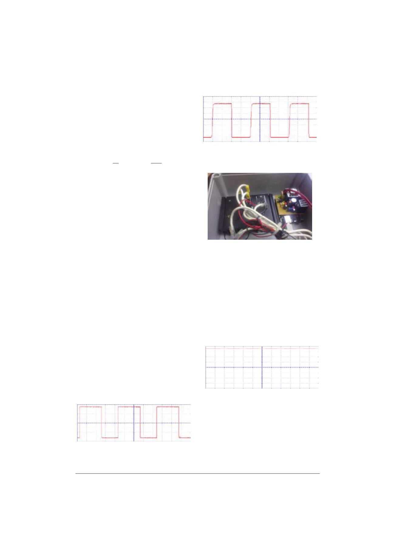
Fig. 5. A prototype of ATmega 328 AVR microcontroller base IGC.
III. E
XPERIMENTAL RESULTS
Based on these design criteria, the laboratory models
of IGC for SEIG have been developed. On the developed
IGC, extensive tests have been performed under steady-
state and transient conditions. Experimentation is carried
out on a three-phase SEIG-IGC system feeding a single-
phase load. The dump load is set as 200 W, in order to
consume the entire consumer load when the chopper duty
cycle is 100%, i.e., when the consumer load is zero. The
consumer load is turned ON and turned OFF alternately
and the output voltage and power are observed to be
constant. The AC voltage and DC voltage experimental
waveforms of the power circuit are show in Fig. 6.
Fig. 6. DC voltage experimental waveforms.
The PID controller parameters are tuned according to
this approach to give the optimal performance. The
terminal voltage is varied between 200 V to 350 V. In
response, the control system will exhibit a corresponding
change in the duty cycle in order to keep the SEIG
terminal voltage constant at the reference value 220 V, as
shown in Fig. 7.


